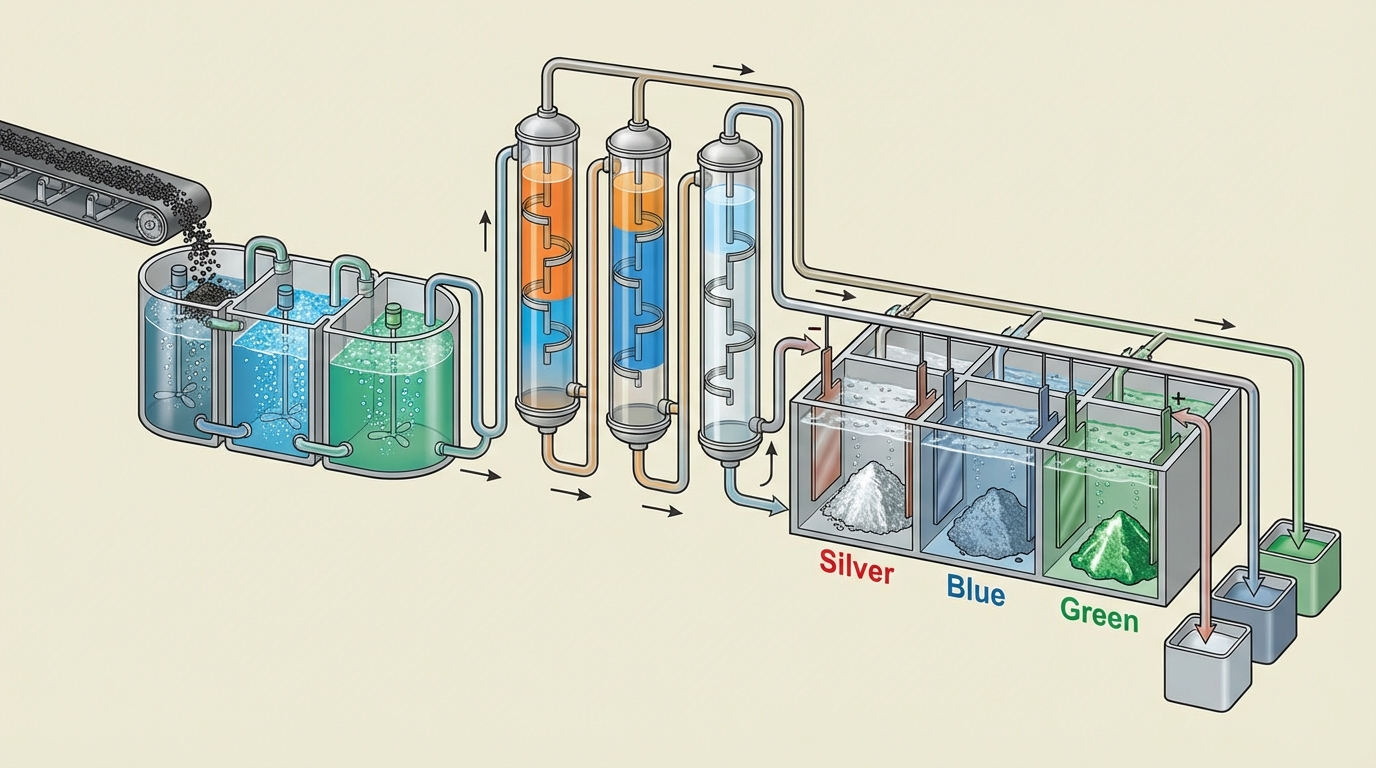
As of August 2026: choose SiC for anything at 800–1200 V and above that must survive heat, surge and 15-year duty — EV traction inverters, solar and storage, industrial drives, grid-side stages of AI data centers; choose GaN for ≤700 V stages where switching frequency and density win — chargers, server power supplies, 800 VDC-to-rack DC-DC, onboard chargers. 1200 V GaN exists in catalogs but is sample/low-volume, so new 900–1200 V designs stay on SiC for now. The supply-risk asymmetry is stark: SiC’s inputs are abundant and its substrates are in Chinese-led over-supply, whereas gallium is ~99% China-produced, Rotterdam prices sit roughly 8–10× the Chinese domestic price (US$1,850–3,050/kg vs ~US$235/kg), and the suspension of China’s US-bound gallium ban expires 27 November 2026.
- Live, dated status of the gallium controls: export-controls tracker · the funded ex-China supply: top 10 non-Chinese gallium and germanium projects · price history: China’s gallium ban · China profile.
GaN or SiC? Decision table by application and voltage class (August 2026)
GaN vs SiC: Why the Choice Hinges on Voltage and Failure Modes
Wide-bandgap (WBG) semiconductors have moved from theory into mainstream power hardware. GaN and SiC devices now sit at the core of EV inverters, onboard chargers, solar inverters, telecom rectifiers, and increasingly, data center power shelves. Underneath the commercial narrative, the physics of gallium nitride and silicon carbide define very different operating envelopes, reliability profiles, and raw-material dependencies. This tech deep dive on gallium nitride vs silicon carbide for power electronics focuses on how the intrinsic materials, device architectures, and supply chains interact to set real limits on what these technologies can credibly deliver between roughly 650-1200 V.
The headline contrast is straightforward: SiC excels when bus voltages and power levels climb, thermal margins tighten, and modules face sustained stress; GaN dominates where switching frequency, power density, and fast transient control are paramount. The reality in production, however, is more nuanced. Gate drive constraints, dynamic loss mechanisms, substrate choices, and gallium availability create second-order effects that are increasingly visible in 2025–2026 hardware platforms — most visibly in NVIDIA’s 800 VDC data-center architecture and in the bifurcated gallium market.
What changed since May 2026
- Markets — Yole (16 Jun 2026): power SiC devices US$3.7bn in 2025 heading to US$11bn by 2031 (~20% CAGR) with upstream utilization near 50% and over-capacity through 2027–28; power GaN ~US$0.58bn (2025) to ~US$3.5bn (2031), TrendForce sees ~US$920m in 2026 (+58%). ST launched seven 700 V PowerGaN HEMTs at US$0.63–2.25 (26 May); onsemi entered GaN with GaNEXUS 40–650 V (8 Jun); Infineon joined the NVIDIA MGX 800 VDC ecosystem (29 May); Navitas pivoted to AI/grid (Q2 revenue US$10.5m); Renesas is closing its Takasaki fab (SiC team dissolved in 2025); TSMC exits GaN foundry by 31 Jul 2027 (licensing to VIS/GF).
- EV — TrendForce (23 Jun 2026): 1.17m SiC traction inverters in Q1 2026 (+7.4% y/y), ~920k of them 800 V-class (+21%) out of 6.82m; Smart #1 (Aug 2026) makes 800 V SiC standard; Changan Qiyuan E07 ships a 650 V GaN 6.6 kW onboard charger (Jul 2026); still no production GaN traction inverter (PCIM, Jul 2026); onsemi cutting up to 300 SiC jobs in Czechia on Chinese price pressure.
- SiC substrates — TanKeBlue’s FY2025 8-inch ASP fell ~60% to ~US$859 with a –105% gross margin (13 Jul 2026); SICC holds 27.6% of conductive substrates and 51.3% of 8-inch; Chinese makers ~40–45% of conductive supply. Wolfspeed emerged from Chapter 11 on 29 Sep 2025 with debt cut ~70%.
- Gallium — CSIS (22 May 2026): the November 2025 truce has not restored meaningful US-bound gallium; Fastmarkets Rotterdam record US$1,850/kg (Apr). SMM: European 6N gallium ~US$2,300–2,350/kg (28 May); a Rotterdam deal at US$2,925/kg for a Japanese buyer (19 Jun); Argus Western benchmark ~US$3,050/kg (30 Jul), about 9× the July 2023 level; China domestic 4N ~US$235/kg on 3 Aug (–18.8% m/m), FOB China ~US$400/kg. Chinese gallium exports: 3 kg in April, 6.2 t in May (6 t to Japan), 200 kg in June (zero to Japan and Germany); H1 ~22.75 t. MOFCOM: enforcement Announcement No. 26 (24 Jun), 20 Japanese entities listed (29 Jun); no relaxation, and the 27 Nov 2026 expiry of the US-ban suspension is unchanged. Alcoa took FID on a ~100 t/yr gallium plant at Wagerup (14 Jul); METLEN signed a US supply deal for 25% of its 50 t/yr Greek output (29 Jul); Neo Performance reported record gallium recycling profit (11 Aug).
- IP — Munich court injunctions against Innoscience GaN products on Infineon patents (18 Jun and 3 Jul 2026); EPC–Renesas licence (11 Feb 2026).
1. Material Fundamentals: Where Physics Sets Absolute Limits
At the foundation, GaN and SiC share the defining attributes of wide-bandgap semiconductors: high breakdown fields, low intrinsic carrier concentrations, and tolerance for elevated junction temperatures. These traits underpin the disruption of traditional silicon IGBTs and MOSFETs. Yet GaN and SiC diverge enough at the material level that they naturally occupy different regions of the voltage–frequency–power map.
1.1 Bandgap, Breakdown Field, and Voltage Headroom
Silicon’s bandgap of around 1.1 eV has long been a bottleneck for high-voltage, high-temperature power electronics. SiC, typically in its 4H polytype, offers a bandgap of roughly 3.2–3.3 eV, while GaN sits slightly higher near 3.4 eV. A wider bandgap suppresses intrinsic carrier concentration by orders of magnitude at a given temperature, which in practice means much lower leakage currents and far higher breakdown fields for the same device geometry.
For SiC, the critical electric field is roughly an order of magnitude higher than silicon. This enables 1200 V and 1700 V MOSFETs and diodes with comparatively thin drift regions and acceptable on-resistance. In EV traction inverters and high-power solar stages, this high breakdown strength translates directly into die area savings or extra margin against overvoltage events and surge conditions.
GaN’s breakdown field is even higher in theory, but the way GaN is realised in power devices constrains that advantage. Most commercial GaN power transistors today are lateral high-electron-mobility transistors (HEMTs) grown epitaxially on foreign substrates (silicon, sapphire, or SiC). The lateral geometry and substrate lattice mismatch make it challenging to scale beyond the 650–900 V class without running into dynamic avalanche, trapping, and long-term reliability concerns. As of 2026, GaN’s volume sweet spot is 100–700 V (and it now reaches down to 15–40 V for 48 V-to-point-of-load stages); nominal 900–1200 V GaN is in catalogs — Innoscience lists 15–1200 V parts, GaNPower stocks a 1200 V e-mode device, onsemi is sampling 1200 V vertical GaN — but remains sample or low-volume and not automotive-qualified, while SiC comfortably covers 650–1200 V and beyond (commercial devices to 3,300 V).
The practical implication: SiC’s bandgap and breakdown field convert into system-level voltage headroom and transient tolerance; GaN’s superior theoretical breakdown field is constrained by device structure and substrate integration rather than the material in isolation.
1.2 Electron Mobility, 2DEG Formation, and Velocity Saturation
The defining feature of GaN in power electronics is the formation of a two-dimensional electron gas (2DEG) at the AlGaN/GaN heterointerface. This 2DEG yields very high electron mobility compared with bulk SiC, typically measured at more than 2000 cm²/V·s in optimised structures, versus around 800–1000 cm²/V·s for 4H-SiC and roughly 1400 cm²/V·s for silicon. Crucially, GaN sustains this mobility at high sheet charge density, enabling low channel resistance and very fast switching.
Both GaN and SiC exhibit high electron saturation velocities, significantly higher than silicon. That trait allows short channels and aggressive scaling of device dimensions without catastrophic mobility degradation at high electric fields. In practice, however, GaN’s heterostructure channel outperforms SiC MOSFET channels at high frequencies. This shows up in device figures of merit that combine on-resistance with charge-related switching losses, where GaN often delivers a lower RDS(on)·QG and RDS(on)·QOSS than similarly rated SiC devices in the sub‑1 kV range.
That mobility edge is the physical reason why GaN can credibly support switching in the MHz range in real power converters, while SiC generally finds its economic sweet spot in the tens to hundreds of kHz range. The cost of that speed is tighter control of parasitics, layout, and gate drive, which becomes a central operational constraint in high-density GaN designs.
1.3 Thermal Conductivity and Heat Flow
Thermal conductivity is one of SiC’s blunt advantages. Bulk SiC is substantially more thermally conductive than silicon, while GaN’s effective thermal performance is heavily influenced by its substrate and epitaxial stack. Typical values cited in industry literature place SiC near several hundred W/m·K, with silicon below that, and GaN on silicon or sapphire even lower once interface resistances are included.
In operational terms, this means SiC devices can sustain higher power densities and junction temperatures before hitting thermal runaway or excessive derating. In traction inverters, where modules are pushed hard under variable cooling conditions, SiC’s ability to maintain safe operation with elevated junction temperatures is often more decisive than a marginal efficiency advantage. Thermal headroom becomes a kind of “safety capital” that can absorb real-world deviations from ideal cooling or load profiles.
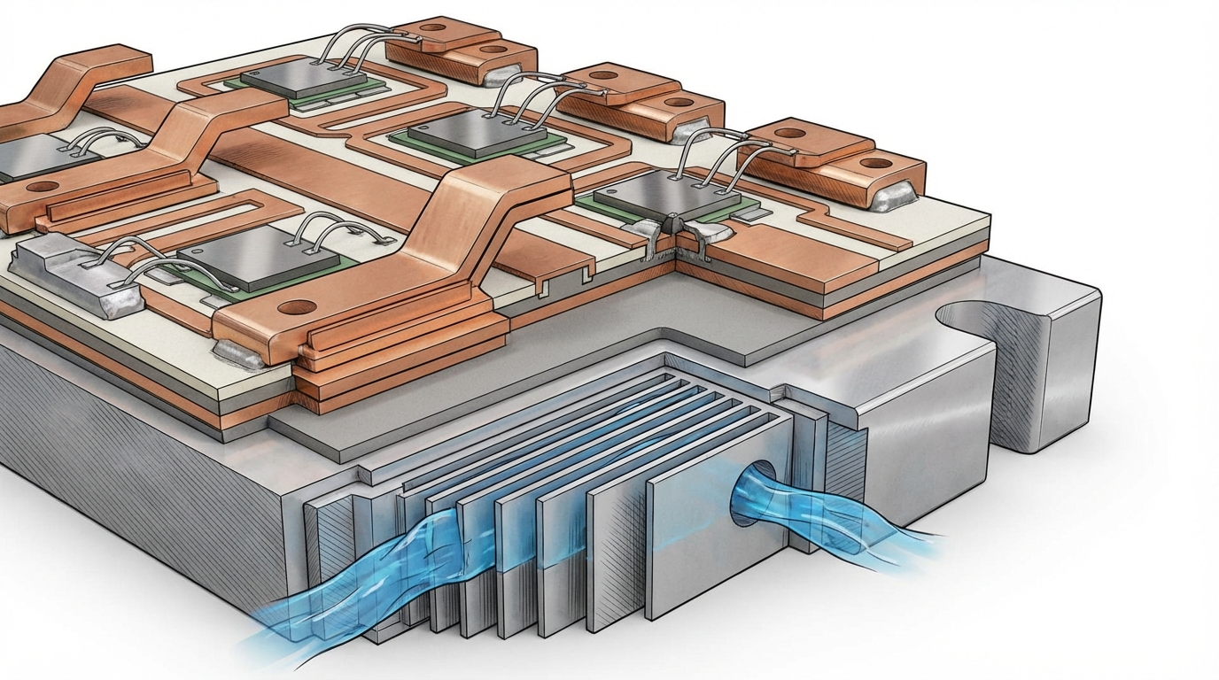
GaN responds differently to thermal stress. GaN devices can exhibit significantly lower switching losses and lower RDS(on) at a given voltage rating, which means that the total heat generated in a given converter stage may be lower than for SiC or silicon. But when localised hotspots do form-especially near the gate or in the buffer-lower substrate thermal conductivity and interface resistance can accelerate local temperature rises. Consequently, GaN’s thermal story is strongly coupled to advanced packaging, careful layout, and often to the adoption of high-performance, low-inductance packages (e.g., embedded packages, laminate-based modules).
| Property (Indicative) | SiC | GaN | Silicon (Reference) |
|---|---|---|---|
| Bandgap | 3.26 eV (4H) | 3.4 eV | 1.12 eV |
| Critical (breakdown) field | ~2.5–3.0 MV/cm | ~3.5–4.0 MV/cm | ~0.25–0.3 MV/cm |
| Typical Power Voltage Range (2026) | 650–1700 V mainstream; 2000–3300 V available | 15–700 V mainstream; 900–1200 V emerging (sample/low-volume) | Up to ~600–900 V |
| Electron Mobility | ~800–900 cm²/V·s (bulk 4H) | ~2,000 cm²/V·s (2DEG) | ~1,400 cm²/V·s |
| Thermal Conductivity | ~3.7–4.9 W/cm·K | ~1.3 W/cm·K (substrate-limited) | ~1.3–1.5 W/cm·K |
| Saturation velocity | ~2×107 cm/s | ~2.5–3×107 cm/s | ~1×107 cm/s |
| Dominant Device Form | Vertical MOSFET/diode | Lateral HEMT (emerging vertical) | Vertical MOSFET/IGBT |
2. Device Architectures and Switching Loss Mechanisms
Material physics alone does not decide outcomes. Device structure, charge storage, and parasitic behavior determine whether those theoretical advantages translate into lower loss and higher reliability in actual converters.
2.1 SiC MOSFETs: Vertical, Rugged, and Thermally Tolerant
SiC power devices are predominantly vertical MOSFETs and diodes. The current path runs perpendicular to the wafer surface, with a thick drift region supporting high voltage and a channel formed under the gate, similar in topology to silicon MOSFETs. This vertical architecture scales naturally to higher voltages by adjusting drift region thickness and doping, at the expense of on-resistance and die area.
SiC MOSFETs still carry some of the limitations of MOS interfaces: channel mobility degradation due to interface traps, threshold voltage shifts under stress, and the need for relatively high gate drive voltages (often in the ±15–20 V range). Their intrinsic body diode also introduces reverse recovery charge, although substantially less than silicon IGBTs. At high switching speeds, charge-related losses in the output capacitance and body diode tail currents begin to dominate, typically constraining economic switching frequencies to a few hundred kHz in high-power applications.
The trade-off is attractive for traction inverters, industrial drives, and large solar inverters: slightly higher switching losses than GaN in exchange for straightforward high-voltage scaling, strong avalanche ruggedness, and robust short-circuit withstand capability when properly derated.
2.2 GaN HEMTs: Lateral 2DEG Channels and Ultra-Fast Switching
GaN power devices are typically lateral enhancement-mode HEMTs. The core conduction channel is the AlGaN/GaN 2DEG, which offers low resistance and high speed. Early devices were depletion-mode, requiring complex gate drive or cascode arrangements; contemporary power GaN generally uses p-GaN or gate-injection structures to create enhancement-mode behavior with gate swings compatible with silicon driver ecosystems.
These devices have two major electrical advantages. First, the absence of an intrinsic body diode eliminates reverse recovery losses. Reverse conduction occurs through the channel itself, which, when properly driven, can significantly reduce Qrr-related losses and EMI. Second, output capacitance and gate charges are typically much lower at a given voltage rating than in SiC MOSFETs. Combined with the high electron velocity in the 2DEG, this translates into extremely short switching times and low ESW at moderate voltages.
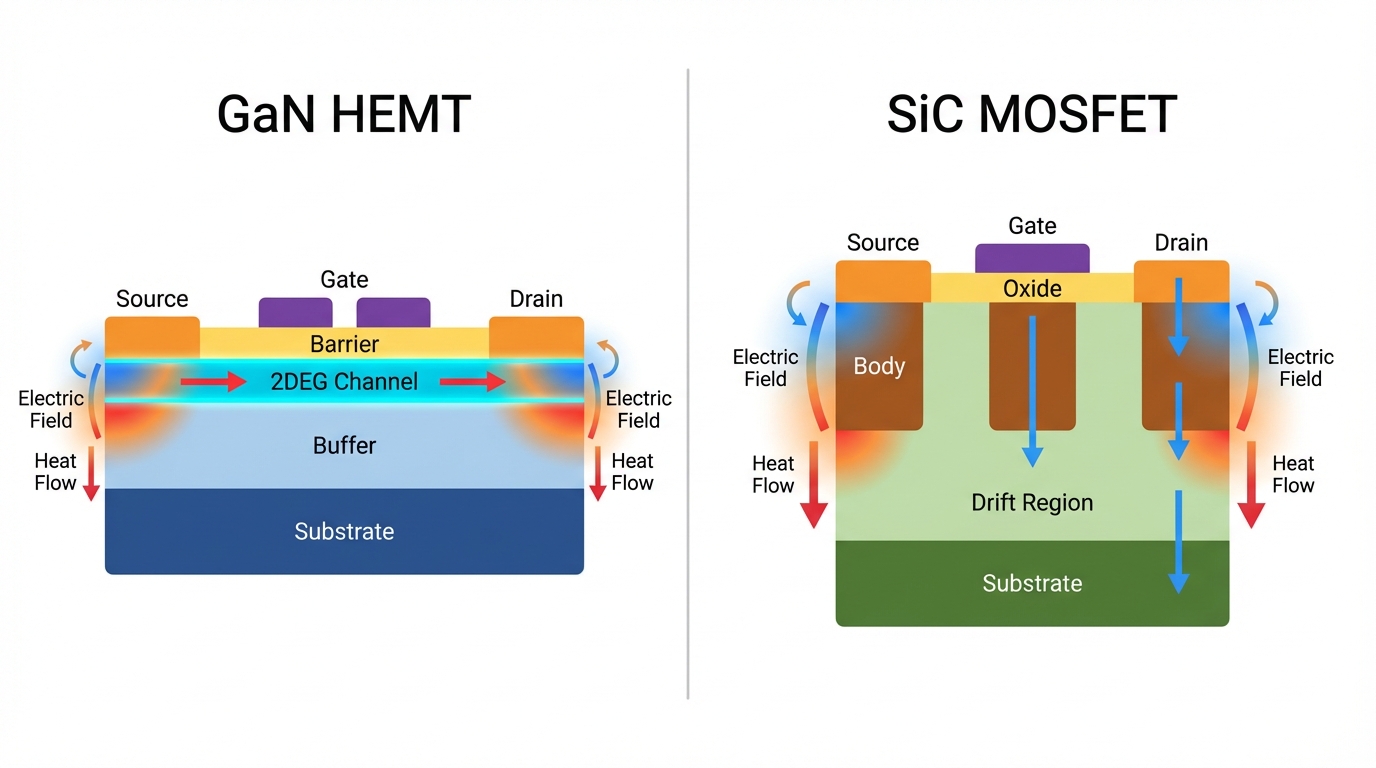
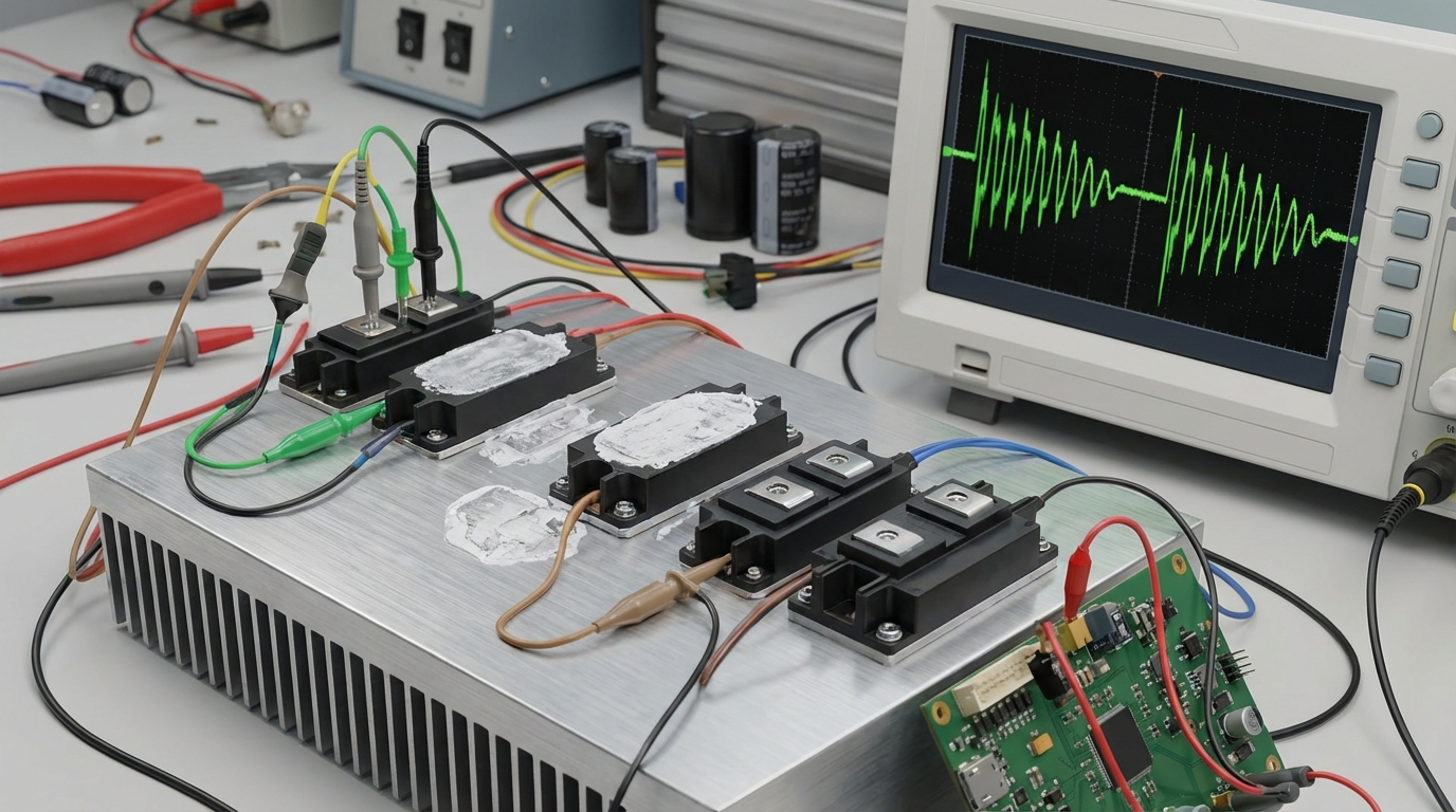
The downside is that such fast switching makes the design hypersensitive to stray inductance, layout, and coupling. Turn-on and turn-off transients can easily create overshoot, ringing, or false triggering if Miller capacitance and gate impedance are not controlled. In other words, GaN’s physics gives access to MHz-class operation, but at the price of much tighter system-level engineering discipline.
2.3 Conduction vs Switching Losses: Where Each Technology Wins
Losses in power devices more or less decompose into conduction losses (I²·R) and switching losses (proportional to V·I·tSW·f). SiC’s lower RDS(on) scaling at high current and high voltage tends to minimise conduction losses in high-power, high-duty-cycle applications. GaN, with its lower capacitances and faster intrinsic dynamics, reduces switching losses dramatically at moderate voltages and currents, especially in hard-switched topologies.
In a high-frequency DC-DC stage or a totem-pole PFC operating below roughly 650 V, GaN frequently yields both higher efficiency and much higher power density by enabling several-fold frequency increases. This shrinks magnetics and reduces the volume of passives. In a 800–1200 V traction inverter, by contrast, SiC’s conduction and surge robustness gains dominate; pushing GaN to equivalent blocking voltages in lateral form would incur unacceptable reliability and derating penalties at current manufacturing maturity.
One analytical insight emerging from field data in 2023–2025 is that SiC’s most valuable contribution in harsh environments is not strictly peak efficiency; it is the enlargement of the safe operating area (SOA). That extra robustness under overvoltage, temperature excursions, and repetitive surge events often determines long-term system behavior more than small percentage-point differences in nameplate efficiency.
3. Reliability, Degradation Mechanisms, and Failure Modes
Reliability physics is where GaN and SiC diverge most clearly. Early failures, long-term drift, and catastrophic breakdown follow different patterns in the two technologies. Understanding these patterns is essential for deciding where GaN and SiC are credible for mission-critical deployments versus where they remain more suitable for consumer or short-lifetime equipment.
3.1 SiC: Channel Instabilities vs Bulk Ruggedness
SiC’s reliability story has evolved rapidly over the last decade. Early-generation devices suffered from significant threshold voltage drift and gate oxide reliability concerns, especially under high-temperature gate bias. Process refinements, improved gate oxides, and defect engineering in epitaxial layers have markedly reduced these issues, but they have not vanished entirely.
Known physics-driven concerns include bipolar degradation (e.g., stacking faults initiated under forward conduction in bipolar devices), basal plane dislocations, and interface trap-related mobility degradation in MOS channels. Modern 4H-SiC processes have largely mitigated the worst effects, and many automotive-qualified devices now demonstrate long mean time to failure (MTTF) even at elevated junction temperatures. Nonetheless, conservative derating, robust gate driver design, and close attention to avalanche limits remain central to SiC reliability engineering.
In return, SiC offers strong avalanche capability and robust short-circuit withstand for carefully specified durations, which is critical for traction inverters and medium-voltage drives. When failures occur, they are often linked to repetitive overvoltage or inadequate thermal design rather than intrinsic material weakness under nominal operating envelopes.
3.2 GaN: Trapping, Dynamic RDS(on), and Buffer Reliability
GaN’s reliability challenges are tied closely to its heteroepitaxial nature and lateral geometry. The AlGaN barrier, GaN buffer, and interfaces to foreign substrates introduce defect populations that interact with hot electrons and high electric fields. Under switching stress, charge trapping in the barrier or buffer can cause dynamic RDS(on) increases—sometimes significant—relative to static datasheet values.
This dynamic RDS(on) rise effectively means that a device operated under realistic high-voltage switching can run hotter and less efficiently than predicted from DC measurements alone. In automotive onboard chargers and industrial PFC stages, this has historically complicated design margins. Newer device generations introduce techniques such as carbon-doped buffers, field plates, and optimised barrier layers to suppress trapping and current collapse, but long-term field data in harsh environments remains more limited than for SiC.
Gate reliability is another focus area. Enhancement-mode GaN HEMTs often operate with relatively narrow gate voltage windows compared with SiC MOSFETs, and are more sensitive to overshoot, undershoot, and oscillations. Tight control of gate driver slew rates, ringing, and Miller coupling is therefore not optional in high-reliability GaN deployments; it is a foundational part of the reliability budget.
3.3 Mission Profiles: Where Field Data Is Converging
Accelerated life testing and field returns increasingly illustrate a pattern. SiC has become the default WBG technology in automotive traction inverters, high-power solar inverters, and other applications where lifetimes of more than a decade under strong thermal and electrical cycling are expected. GaN has become the technology of choice in fast chargers, laptop and phone adapters, compact server power supplies, and telecom rectifiers, where operating voltages are lower and mission lifetimes, while still significant, are less extreme than in grid or traction hardware.
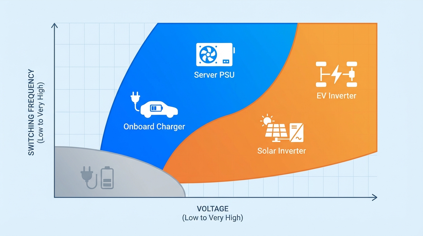
A key emerging observation is that GaN can achieve silicon-like or better reliability in consumer and datacom-grade conditions, provided that gate driving and thermal design are executed with tight control. In heavy-duty industrial or transportation environments with wide ambient swings, high surge exposures, and complex EMC/EMI constraints, SiC retains a structural advantage stemming from its vertical device geometry and bulk material robustness.
4. Application Mapping: Where GaN and SiC Compete or Complement
On paper, both GaN and SiC can serve across a wide power and voltage range. In practice, economics, packaging, and reliability push the technologies into partially overlapping but distinct application domains.
4.1 EV Powertrains and High-Voltage Mobility
EV traction inverters at 800 V class and above are now heavily associated with SiC. The combination of 1200 V rated MOSFETs, high thermal conductivity, and strong avalanche behavior aligns well with the needs of traction drives subjected to repetitive load cycling, harsh vibration, and non-ideal cooling. SiC enables significant reductions in conduction loss compared with silicon IGBTs, supports compact motor inverters, and simplifies cooling system design in many architectures. The numbers as of mid-2026: TrendForce counted 1.17 million SiC-based traction inverters in Q1 2026 (+7.4% year-on-year) out of 6.82 million, with ~920,000 of them on 800 V-class platforms (+21%); Smart’s #1 made 800 V SiC standard in August 2026. Two caveats: Tesla’s 2023 decision to cut SiC content per vehicle by ~75% still shapes device-count assumptions, and SiC is in over-supply — Yole puts upstream utilization near 50% with the glut lasting into 2027–28, ST and onsemi have reported softness, and 8-inch substrate prices have collapsed (TanKeBlue’s FY2025 8-inch ASP ~US$859, down ~60%).
GaN’s current role in EVs is more concentrated in onboard chargers (OBCs), DC-DC converters, and auxiliary power supplies. In those subsystems, especially below 650 V, GaN’s high switching frequency capability allows substantial reductions in magnetics and passive components, enabling lighter and more compact power electronics. Some EV platforms combine SiC-based traction inverters with GaN-based onboard chargers, effectively splitting the powertrain according to voltage and mission profile: Changan’s Qiyuan E07 ships a 650 V GaN 6.6 kW onboard charger (July 2026), Infineon reports design wins in OBCs, and PCIM 2026 confirmed there is still no production GaN traction inverter.
4.2 Renewables, Storage, and Grid-Tied Equipment
Large solar string inverters, central inverters, and utility-scale storage systems place a premium on high-voltage handling, surge robustness, and long lifetimes in challenging outdoor environments. SiC has gained traction here for similar reasons as in traction drives: the ability to handle 1000–1500 V DC buses, strong thermal characteristics, and credible 15–20 year lifetime expectations under field conditions.
GaN’s presence in renewables is more visible in lower power stages, such as module-level power electronics (MLPE), residential-scale inverters, or auxiliary DC-DC converters where footprint, efficiency at partial loads, and high-frequency operation are decisive. The combination of compact magnetics and high switching speeds can materially reduce the size and weight of rooftop or wall-mounted gear, though long-term field performance data in these outdoor environments is still accumulating.
4.3 Data Centers, Telecom, and Consumer Fast Charging
This is where GaN’s device physics is most fully exploited, and where the 2026 story has moved fastest. The old frame was 48 V bus conversion; the new one is NVIDIA’s 800 VDC rack architecture (MGX), which pushes GaN into the 800 V→50/12/6 V stages: Navitas demonstrated a 10 kW 800→50 V all-GaN platform at 1 MHz and 98.5% peak efficiency (February 2026) and a 20 kW 800→6 V stage at 97.5% (May); ST fielded a 6 kW power-distribution board on 700 V GaN; Infineon joined the MGX 800 VDC ecosystem on 29 May 2026 with silicon, SiC and GaN “grid-to-core”; Innoscience won an NVIDIA supplier award (19 March) and a Google design-in (February). SiC takes the grid-side solid-state transformer and active-front-end stages (1200–3300 V) and hot-swap protection; onsemi says its SiC data-center revenue is up ~60% in 2026. Reducing inductor and transformer size, often by double-digit percentages, has direct consequences for rack-level power density and airflow, and GaN’s partial-load efficiency aligns with real server utilisation profiles.
In consumer fast chargers and adapters, GaN has already redefined form factors, allowing tens to hundreds of watts of power in extremely compact packages. Here, the controlling constraints are cost, safety, and thermal comfort rather than 15–20 year lifetimes, and GaN’s physics aligns almost perfectly with the design space.
SiC is not absent in datacom or fast-charging ecosystems, but its cost structure and advantages are more attractive at higher voltages and powers than those encountered in consumer adapters or rack-level DC-DC. With 700 V GaN HEMTs now priced at roughly US$0.63–2.25 in volume (ST, May 2026) and at least six merchant suppliers, GaN is structurally advantaged — and commoditizing — across much of this segment.
5. Gallium vs Silicon Carbide: Raw Materials, Wafer Technology, and Supply Risk
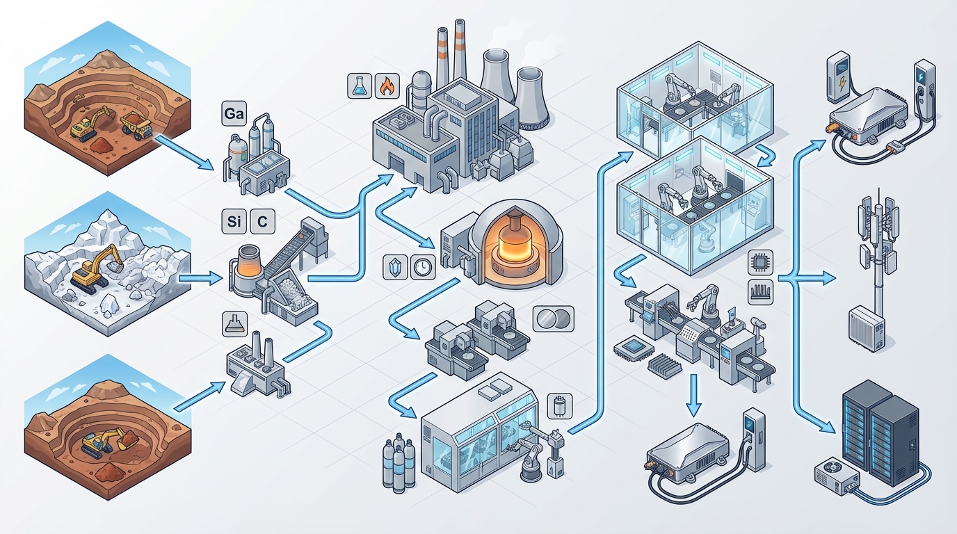
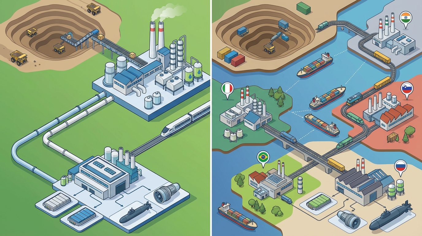
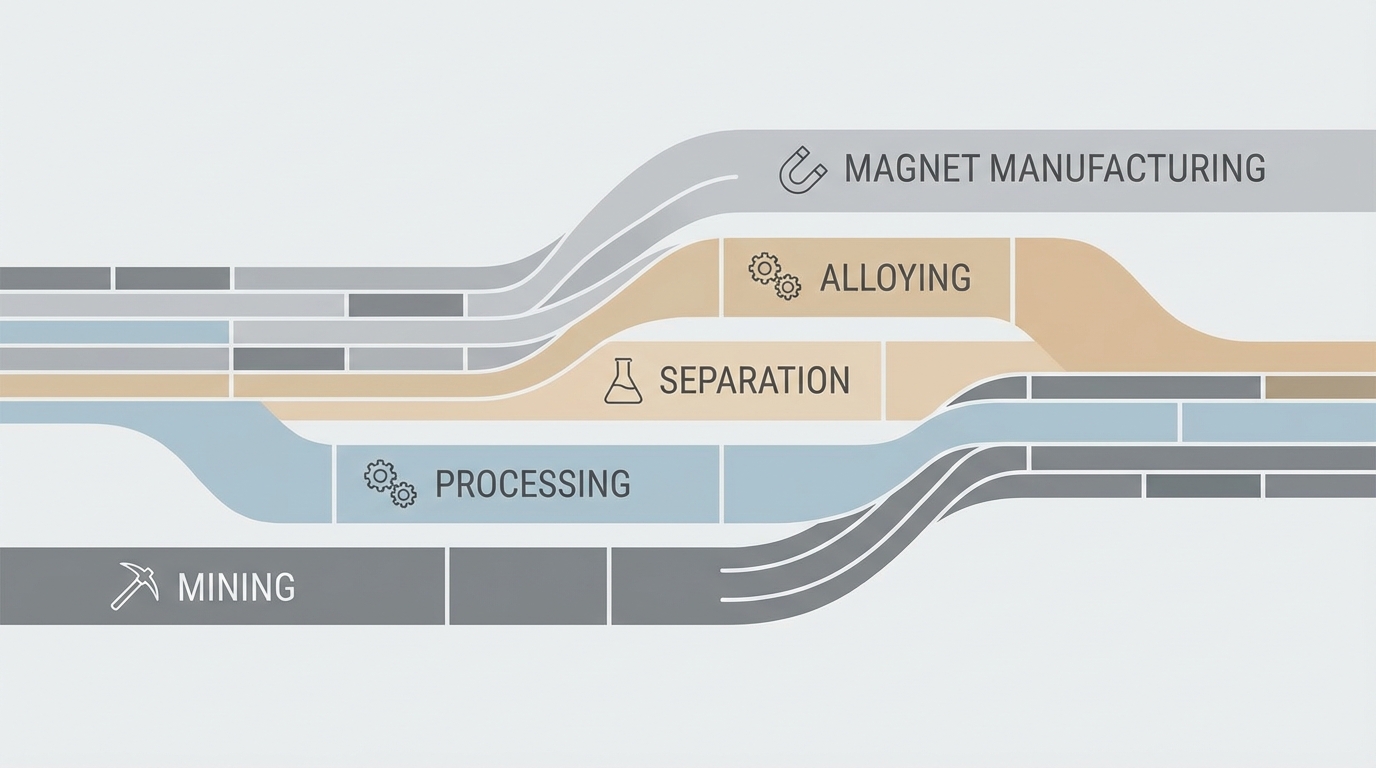
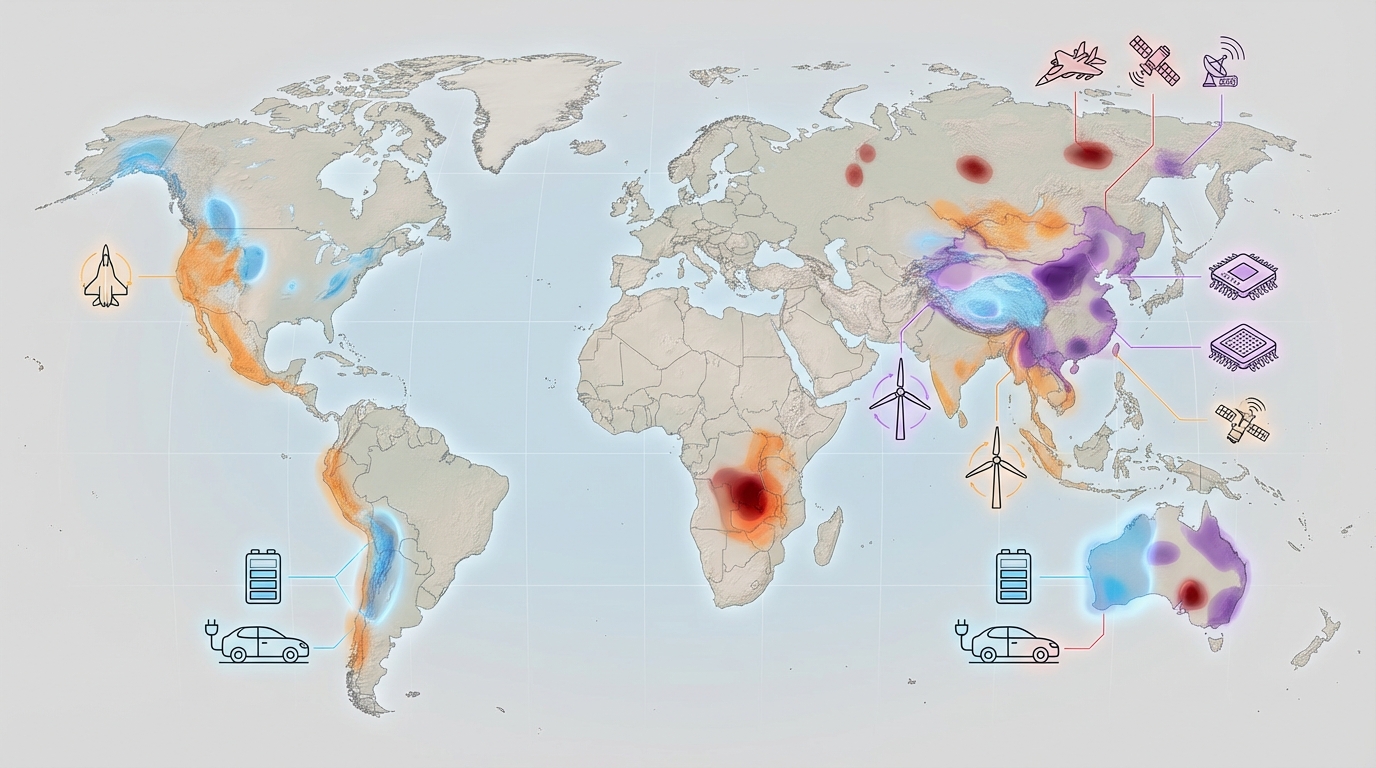
From a materials and mining perspective, GaN and SiC are not equal. The gallium needed for GaN devices is produced almost entirely as a by-product of other mining and refining operations, while silicon and carbon for SiC are derived from far more abundant and geographically diversified sources. This asymmetry is central to understanding strategic risk profiles during rapid WBG adoption, traced in detail in our wide-bandgap supply chain deep dive.
5.1 Gallium: By-Product Dependency and Concentrated Refining
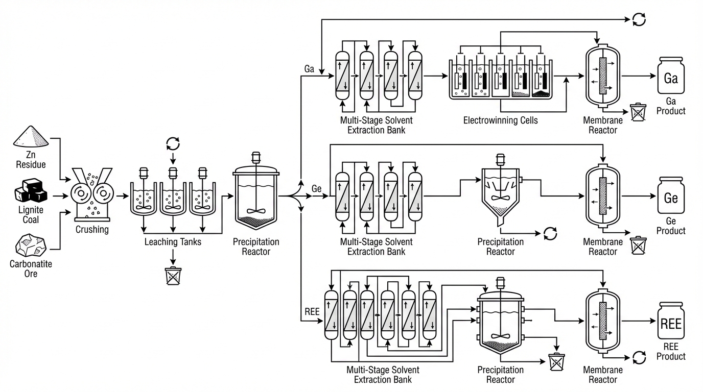
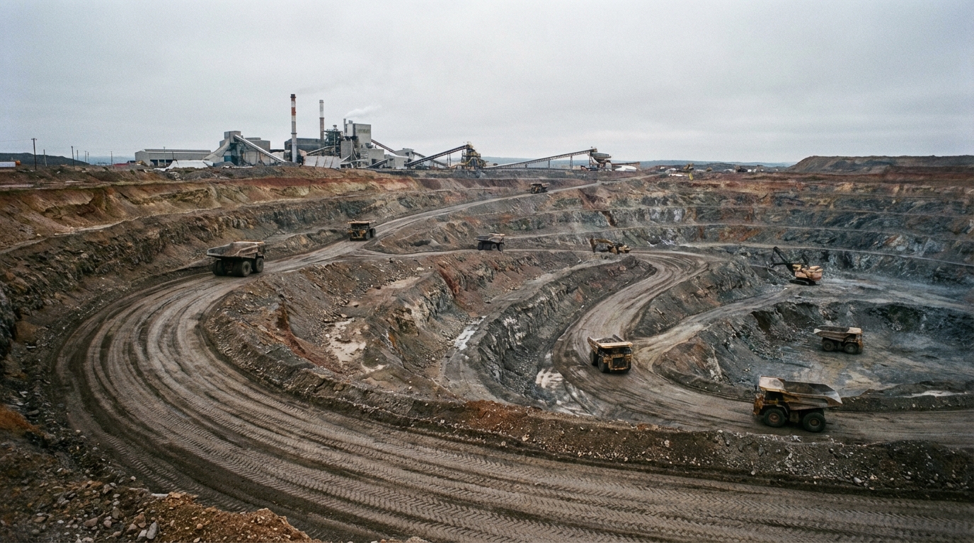
Gallium is typically recovered as a minor constituent from bauxite processing (alumina refineries) and from certain zinc processing streams. Because gallium production is tied to aluminium and zinc output, primary supply is relatively inelastic to demand from LEDs and power electronics. Refined gallium production is extraordinarily concentrated: the USGS Mineral Commodity Summaries 2026 put 2025 world primary low-purity gallium at ~900 t, essentially all of it (~99%) from China, with China holding ~1,600 t of the world’s ~1,700 t of capacity. Western buyers depend on a thin set of non-Chinese gallium and germanium sources — the funded pipeline as of August 2026 is Alcoa’s ~100 t/yr Wagerup plant (FID 14 July 2026, first output targeted 2027), METLEN’s 50 t/yr plant in Greece (2027–28), Rio Tinto’s Quebec pilot (up to 4 t/yr in 2027, 40 t/yr option), Korea Zinc’s Tennessee smelter (~2029–30) and Neo’s recycling — none of which delivers before 2027.
The controls are specific and dated. China placed gallium under dual-use export licensing on 1 August 2023, announced a US-specific export ban on 3 December 2024 (Announcement No. 46), and on 9 November 2025 suspended that ban until 27 November 2026 (Announcement No. 72) — the worldwide licence requirement and the ban on exports to US military end-users never lapsed, and as of 16 August 2026 the MOFCOM register shows no relaxation. Beijing added Japan-specific restrictions in January 2026 and listed 20 Japanese entities on 29 June, and its enforcement Announcement No. 26 took effect on 1 July. The result is a bifurcated market: SMM quoted China domestic 4N gallium at ~US$235/kg on 3 August 2026 (FOB China ~US$400/kg), while Fastmarkets recorded a Rotterdam high of US$1,850/kg in April, European 6N traded ~US$2,300–2,350/kg in late May, and Argus assessed a Western benchmark near US$3,050/kg on 30 July — roughly nine times the July 2023 level. Chinese customs show gallium exports of 3 kg in April 2026, 6.2 t in May (6 t to Japan) and 200 kg in June (zero to Japan and Germany), ~22.75 t for the half-year. For GaN power electronics, this concentrates upstream exposure: even if epitaxy, wafer processing, and device fabrication are geographically diversified, the gallium-bearing feedstock still often originates from a small cluster of refineries. Under frameworks such as the EU Critical Raw Materials Act and related national regulations, this has already driven tighter scrutiny of material provenance, long-term offtake contracts, and recycling potential from LED and RF waste streams.
5.2 Silicon Carbide: Abundant Precursors, Complex Crystals
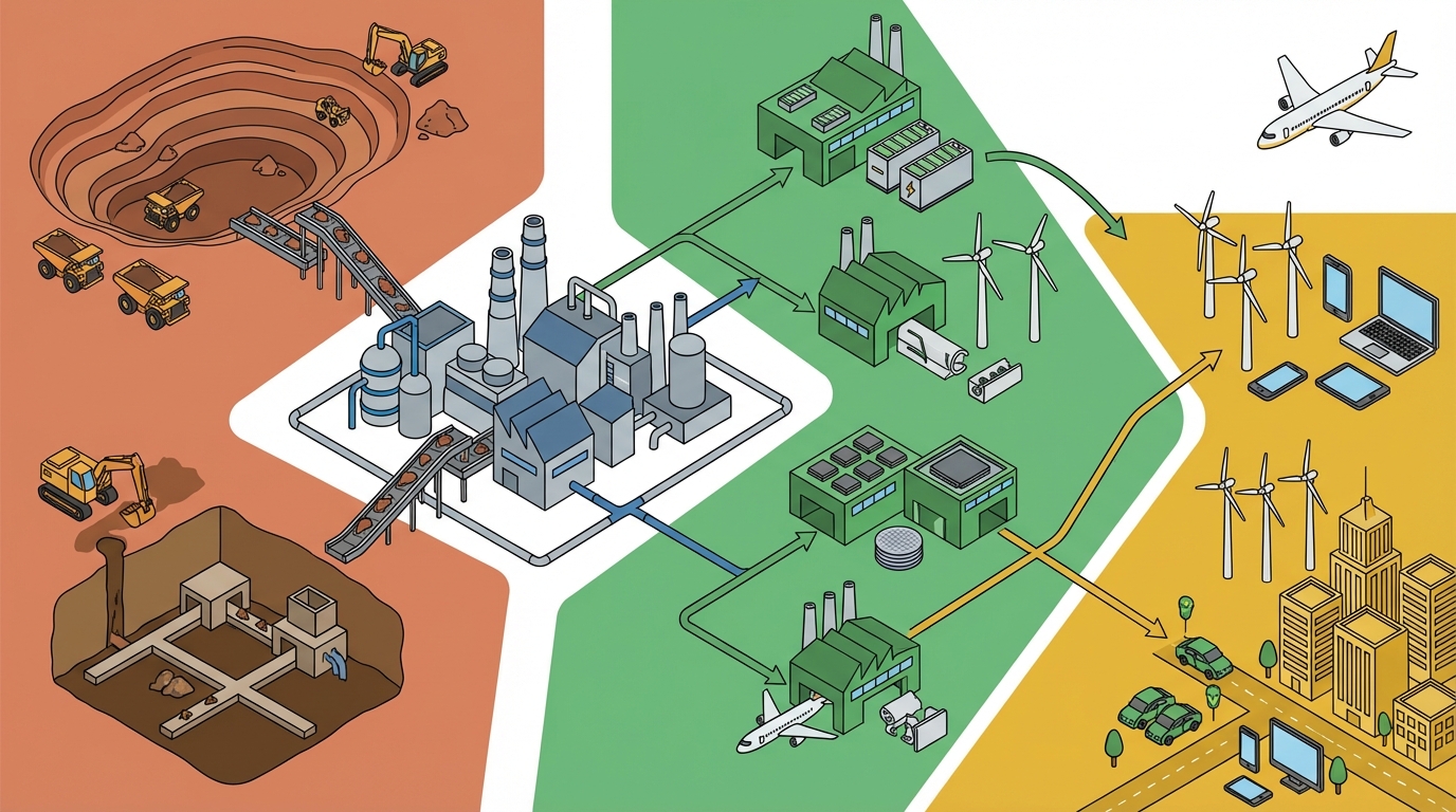
SiC draws on far more abundant raw materials: high-purity quartz or silica, metallurgical-grade silicon, and carbon sources such as petroleum coke or other high-purity carbons. The strategic constraint is not geological scarcity, but rather the complexity of growing large, defect-controlled SiC boules and wafers. Physical vapor transport (PVT) crystal growth is capital- and energy-intensive, and scaling from 150 mm to 200 mm wafers has been a major area of industrial focus.
This means SiC supply risks are more about manufacturing capacity, yield, and process control than raw ore availability — and, in 2026, about who owns the substrate business. Chinese conductive-substrate makers now hold roughly 40–45% of global supply (SICC 27.6% overall and 51.3% of 8-inch in 2025), 8-inch is the benchmark, and a price war has pushed TanKeBlue’s 8-inch ASP to ~US$859 (–60%) with negative gross margins; Western supply is financially fragile (Wolfspeed filed Chapter 11 on 30 June 2025 and emerged 29 September with debt cut ~70%; Renesas abandoned SiC; JS Foundry went bankrupt in July 2025). From a critical materials standpoint, SiC still sits in a more comfortable position: it does not depend on a single-country by-product stream, its precursors are widely distributed, and buyers face a glut rather than a squeeze — the risk is supplier concentration and viability, not ore.
5.3 Wafer and Epitaxy Ecosystems
On the midstream side, GaN and SiC require different infrastructure. SiC wafers are grown as bulk single crystals, sliced, and polished before epitaxial layers are deposited. Wafer sizes have historically lagged silicon, but 150 mm and 200 mm wafers are now standard targets, with some pilot efforts exploring larger diameters. Tooling, epitaxy reactors, and fab processes are increasingly tuned specifically to SiC device structures.
GaN power devices, by contrast, are usually realised as GaN epitaxial layers grown on silicon or SiC substrates using metal-organic chemical vapor deposition (MOCVD) or related techniques. This allows reuse of large-diameter silicon wafers and partially leverages existing silicon fab lines — though the foundry map is shifting: TSMC exits GaN foundry by 31 July 2027 (licensing to VIS and GlobalFoundries), Samsung is entering, Innoscience runs an 8-inch GaN-on-Si IDM, and EPC licensed Renesas in February 2026 — but at the cost of managing thermal expansion and lattice mismatch between GaN and the substrate. These mismatches drive dislocation densities and defect structures that feed directly into trapping, leakage, and long-term reliability.
Vertical GaN on native GaN substrates is an area of active development aimed at high-voltage applications, promising to combine GaN’s superior breakdown field with vertical architectures akin to SiC. The limiting factor is currently the availability and cost of high-quality bulk GaN substrates, which are even more challenging to produce at scale than SiC boules. This emerging path is strategically important but not yet a volume alternative to SiC at 1200 V and above.
6. Implementation Realities: Gate Drive, Packaging, and Compliance
Even where physics clearly favours GaN or SiC for a given application, implementation constraints can override theoretical advantages. Gate drive ecosystems, package standards, EMC compliance, and qualification requirements all shape which technology is credible in a given sector.
6.1 Gate Driving and Control Electronics
SiC MOSFETs typically require relatively high gate voltages with defined positive and negative drive levels (for instance, +15/−5 V ranges are common), and tolerate relatively slower switching speeds while still delivering efficiency gains over silicon. Gate drivers need sufficient immunity to high dV/dt environments and robust desaturation protection, but the overall design language is a natural extension of high-voltage silicon MOSFET experience.
GaN gate driving is more delicate. Enhancement-mode HEMTs often operate with small gate voltage windows, and are intolerant of overshoot beyond specified limits. Fast transients, high dV/dt, and strong Miller coupling require carefully matched drivers, short gate loops, and sometimes integrated driver–FET packages to manage parasitics. In many of the highest-density GaN designs, successful operation depends as much on co-packaged drivers and optimised layouts as on the intrinsic device physics.
6.2 Packaging, Layout, and EMI
SiC modules for traction and industrial drives often adopt standard power module formats, sometimes shared with silicon IGBTs, easing mechanical integration but not always optimising loop inductances. Even so, switching speeds relative to silicon are sufficiently higher that package and layout parasitics still receive far more scrutiny than in legacy designs. Co-optimised module layouts, press-fit terminals, and low-inductance busbars are now standard in advanced SiC power stacks.
GaN’s very fast edges and high frequency potential strongly incentivise packages with minimal parasitic inductance and capacitance: embedded packages, chip-scale packaging, and laminate-integrated solutions are common. These design choices materially affect EMC and conducted/radiated emissions. Inadequate attention to PCB stack-up, return paths, and common-mode chokes can quickly erode the theoretical efficiency gains from GaN by forcing derating or additional filtering.
6.3 Standards, Qualification, and Industrial Resilience
Automotive and grid equipment impose rigorous qualification chains: AEC-Q101 for discrete semiconductors, ISO/TS standards, and various JEDEC specifications. SiC devices now have a visible track record in meeting these requirements, and several leading SiC vendors have dedicated automotive-qualified lines. This maturity feeds back into design decisions, as OEMs can rely on accumulated field data and structured failure analysis.
GaN devices have achieved automotive qualification in selected categories, but deployment remains more concentrated in consumer, datacom, and selected industrial roles. Qualification cycles continue to extend into more demanding mission profiles, yet many OEMs still view GaN as a younger technology for high-voltage, long-lifetime applications. From an industrial resilience perspective, this means SiC currently anchors more of the long-life, safety-critical nodes in the global power electronics infrastructure, while GaN increasingly populates high-density but shorter-lifetime equipment.
What to do now, by role (August 2026)
7. Trade-Off Synthesis: Physics, Risk, and Material Constraints
Aggregating these layers—physics, device architecture, reliability, and supply chains—reveals a clearer structural picture of GaN vs SiC in power electronics.
First, SiC is structurally advantaged wherever high voltage, high power, and harsh operating conditions coincide. Its vertical architecture, high breakdown field, and thermal conductivity create a large safety margin. That margin is what supports 800 V traction inverters, utility-scale solar, and industrial drives that need to survive decades of cycling, overloads, and non-ideal cooling.
Second, GaN is structurally advantaged where switching frequency, power density, and form factor dominate the requirements, and where mission profiles are compatible with tightly controlled gate drive and thermal design. Datacenter power supplies, telecom rectifiers, and consumer fast chargers are the clearest examples. In these environments, GaN transforms magnetics, enclosure size, and thermal management assumptions, often achieving both higher efficiency and substantial size reductions versus silicon or even SiC at equivalent voltages.
Third, material supply chains tilt risk profiles in different directions. Gallium’s by-product status, ~99% Chinese primary production, licence-gated exports and an 8–10× price gap between China and Rotterdam elevate geopolitical and regulatory risk for GaN, even as more epitaxy and device fabrication capacity moves into diversified geographies. SiC, anchored in abundant silicon and carbon sources but with substrates now in Chinese-led over-supply, presents a supplier-viability and concentration question rather than a raw material risk. These differences matter for governments, OEMs, and regulators planning long-term electrification and digital infrastructure.
Finally, overlap zones are substantial. Onboard chargers, residential solar inverters, industrial power supplies, and mid-power drives sit in a regime where both GaN and SiC can credibly compete. In these spaces, selection often hinges on institution-specific comfort with each technology’s failure modes, internal design capabilities for high-speed switching, and sensitivity to raw material risk and regulatory oversight.
From the Materials Dispatch perspective, the decisive insight is this: in WBG power electronics, the key variable is not which material is “better” in the abstract, but which combination of physics, packaging, and supply chain constraints is acceptable at each node of the power conversion stack. As EV architectures, renewable penetration, and data center loads continue to escalate, active monitoring of gallium policy signals, SiC wafer capacity expansions, and reliability field data will define how the GaN–SiC balance evolves in the coming hardware cycle.
Note on Materials Dispatch methodology Materials Dispatch integrates technical literature on WBG device physics, regulatory and trade monitoring around critical materials (such as gallium), and market data on end-use specifications in EVs, renewables, and datacenters. This cross-reference of process-level engineering constraints with upstream material realities underpins the assessments presented in this analysis.
Sources
- STMicroelectronics — AN5583, E-mode GaN technology: tips for best driving (material parameters) — st.com
- Yole Group via Compound Semiconductor — Power SiC enters the AI age — 16 Jun 2026 — compoundsemiconductor.net; DQ India — Power SiC faces overcapacity downturn — 1 Jan 2026 — dqindia.com
- TrendForce — Q1 2026 traction inverter and SiC installations — 23 Jun 2026 — trendforce.com; TrendForce — TSMC licenses GaN technologies to VIS and GF — 2 Feb 2026 — trendforce.com
- HDIN Research — TanKeBlue FY2025 8-inch substrate ASP — 13 Jul 2026 — hdinresearch.com
- Financier Worldwide — Wolfspeed emerges from Chapter 11 — 2 Oct 2025 — financierworldwide.com
- Infineon — Infineon joins NVIDIA MGX 800 VDC ecosystem — 29 May 2026 — infineon.com; Navitas — 10 kW 800 V→50 V GaN platform at 98.5% — 9 Feb 2026 — navitassemi.com; onsemi — GaNEXUS launch — 8 Jun 2026 — onsemi.com
- PCIM / Mesago — SiC vs GaN in 2026 and beyond — 29 Jul 2026 — news.pcim.mesago.com
- USGS — Mineral Commodity Summaries 2026: Gallium — pubs.usgs.gov
- CSIS — The U.S.-China trade truce has not solved the gallium problem — 22 May 2026 — csis.org
- SMM — Ex-China high-purity gallium prices continue to rise sharply — 28 May 2026 — metal.com; SMM data via rare-earth-mining.com — Gallium price today — 3 Aug 2026 — rare-earth-mining.com
- Reuters — China’s heavy rare earth tap stays closed for Japan in June (gallium 200 kg) — 20 Jul 2026 — reuters.com
- Reuters — Alcoa greenlights Australia gallium plant with US, Japan, domestic backing — 14 Jul 2026 — reuters.com; METLEN — Landmark gallium supply agreement — 29 Jul 2026 — metlen.com; Rio Tinto — Gallium metal R&D project with the Government of Canada — 2 Mar 2026 — riotinto.com
Caveats: the ~US$3,050/kg Argus figure is cited via secondary market reports (Fastmarkets/Argus series are paywalled) — treat US$1,850/kg (April, CSIS) as the hard record and US$2,300–3,050 as reported June–July trades; SiC vendor-share percentages are secondary compilations of Yole/TrendForce data.